Every microfluidics experiment faces the same problem: connecting a delicate chip to real-world equipment. A custom microfluidic chip fixture solves this chip-to-world interface issue. It holds your device securely while giving leak-free fluidic access. Success depends on four key parts: requirements analysis, design engineering, material science, and fabrication & assembly.
Are leaks, misalignment, or dead volume hurting your microfluidic work? This practical guide tackles those challenges for research prototypes and production systems alike. We’ll look at each part with engineering-focused advice for your microfluidic setup. Companies like NOBLE offer manufacturing skills for microfluidic chip fixture prototyping and production. Their precision machining supports your microfluidic chips from idea to deployment. Let’s start.
Microfluidic Chip Fixture Requirements
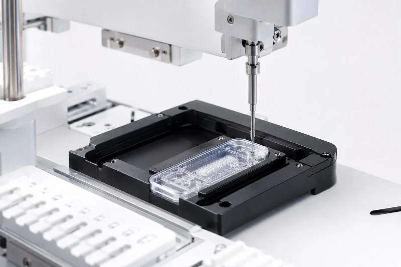
Before you open CAD software or buy materials, you need to know exactly what your chip needs. The fixture must fit the chip’s material—PDMS, glass, or thermoplastics—and match how that material was made. A PDMS chip bonded to glass acts differently in size and shape than a molded thermoplastic part. Knowing this history helps you avoid expensive redesigns later.
Your microfluidic chip fixture does two jobs. First, it lines up chip layers during bonding. Second, it holds the finished device for fluid connections. Both jobs need the same level of accuracy. Start by collecting your chip datasheet, CAD files, and any fabrication notes. This list becomes your design base.
Analyzing Chip Dimensions and Geometry
Measuring Critical Tolerances
Chip sizes change more than most researchers expect. Soft lithography causes shrinkage when PDMS cures. Glass etching creates depth differences across features. Measure your real chips, not just the CAD numbers. Use a calibrated microscope or coordinate measuring machine for this step.
Standard size tolerance for microfluidic chip fixtures reaches 10 μm or less. Getting this requires tools in a temperature-controlled room kept at ±0.1 °C. Heat changes alone can push you past acceptable limits. If your lab lacks this setup, include that in your tolerance plan. NOBLE’s engineering skills help study chip sizes and pick the right connections for your microfluidic chip fixture.
Identifying Port Locations and Pitch
Port placement decides where your microfluidic chip fixture must touch the chip. Measure the center-to-center distance between nearby ports—this pitch guides your manifold design. Also write down port diameter and depth. A port that sits below the chip surface needs a different sealing method than one level with the top.
Record these numbers in a table. Include tolerances for each measurement. When you design the microfluidic chip fixture, every hole and channel uses these numbers. Small mistakes here grow through the whole assembly.
Determining Fluidic Interface Needs
Selecting Connector Types (Luer, Ferrule, etc.)
Your connector choice depends on working pressure and tubing preferences. The table below shows common options:
| Connector Type | Pressure Rating | Additional Context |
| Capillary tube interface | Up to 1000 psi (70 bar) | Made for high-pressure liquid chromatography; fits tough microfluidic uses |
| Luer fitting (per ISO spec) | 43.5 psi (300 kPa) | Tested per ISO 80369-7 when set up correctly |
| Luer with barb adapter | May be lower than 43.5 psi | Working pressure depends on barb/tubing mix with soft elastomer tubing |
Match the connector to your experiment’s real pressure needs. Over-specifying adds cost. Under-specifying causes leaks.
Calculating Dead Volume Constraints
Dead volume—the fluid stuck between your chip and your tubing—dilutes samples and widens peaks. For complex test protocols, this matters a lot. Reduce dead volume by keeping fluid paths short and inner diameters small. Calculate the volume of each channel section in your fixture. Add these values. Compare the total against your assay’s limit for sample spreading.
Assessing Application-Specific Constraints
Temperature and Pressure Ranges
Your fixture must handle your experiment conditions. If you run reactions at high temperatures, the microfluidic chip fixture material must match your chip’s heat expansion. Otherwise, the seal fails as temperatures rise. Likewise, pressure cycling wears down materials over time. Write down your maximum working pressure and temperature before picking materials.
Optical Access for Imaging and Detection
Many microfluidic experiments need microscopes. Your microfluidic chip fixture must not block the light path. Plan viewing windows or clear sections early in the design. A metal fixture with a cut-out opening works well for transmitted light. For fluorescence detection, think about the working distance of your lens. The fixture thickness directly affects this setting.
Design Principles for Custom Microfluidic Devices

Your design phase must handle two jobs at once. It needs to support the chip’s making process—like lining up layers during PDMS-glass bonding—and it must work well during real experiments. A microfluidic chip fixture that fails at either point will cause issues. NOBLE offers design review and optimization services for microfluidic chip fixtures to help you catch these problems early. The key is to design for even pressure during bonding and to avoid features that are hard to machine or mold.
CAD Modeling and Tolerance Stack-Up
Tolerance stack-up affects every part of your microfluidic setup. Small errors in chip dimensions add up. A PDMS chip that shrinks by 1% during curing might still fit in a pocket made for the normal size. But that same 1% shift plus a 0.2mm port misalignment can cause a leak. Run a tolerance stack-up analysis early. This checks every dimension layer by layer.
At Ascential, we combine DFM analysis, tolerance stack-ups, and process development with product design. The result is instruments that keep accuracy, throughput, and reliability from prototype to clinical and commercial production.
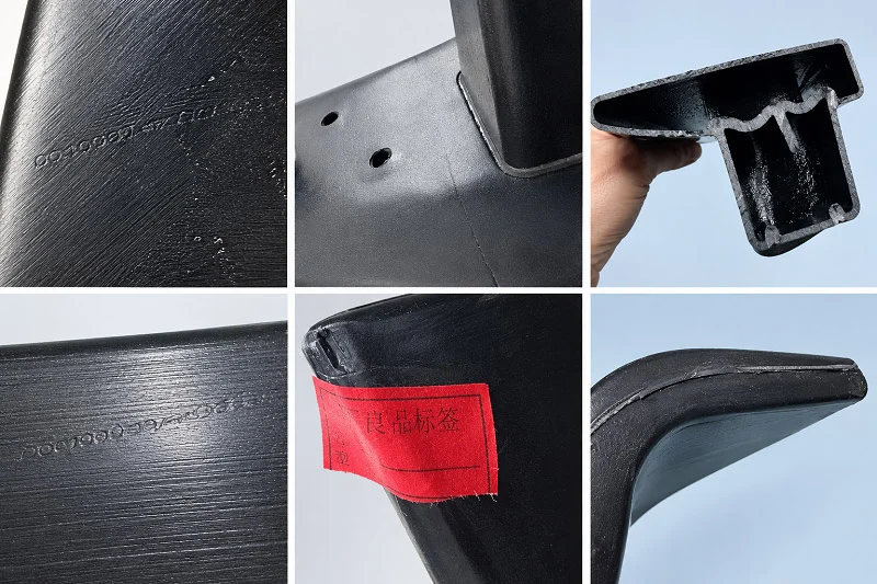
A chip that works well in small-batch testing may still fail during mass production due to: bonding variation, material batch inconsistency, mold wear over time, assembly tolerance stack-up, surface treatment instability, and thermal deformation after storage or transport.
These quotes show why tolerance matters. Your design must account for real-world variation, not just perfect CAD numbers.
Designing for Press-Fit vs. Slip-Fit
Press-fit holds the chip tight. It works when your chip dimensions are very consistent. Slip-fit gives room for the chip to move. It works better when chip sizes vary. Most microfluidic fixtures use a slip-fit with a small gap. A clearance of 0.1mm to 0.2mm on each side lets the chip sit without stress. Alignment features then guide it into place.
Accounting for Material Thermal Expansion
Different materials expand at different rates. PDMS expands more than glass. Aluminum expands more than PEEK. If your fixture and chip expand at different rates, the seal can break when temperature changes. Calculate the thermal expansion for your temperature range. Make sure the chip pocket and sealing surfaces stay aligned at both low and high temperatures.
Implementing Alignment Features
Alignment features make sure your chip sits in the right spot every time. Without them, port alignment changes with each setup. This causes leaks and inconsistent results.
Using Dowel Pins and Alignment Slots
Dowel pins give a fixed reference point. Place two pins on one edge of the chip pocket. The chip touches both pins when you insert it. An alignment slot on the opposite edge lets the chip expand without buckling. This setup centers the chip over the ports every time you use the fixture.
Creating a Chip Nest or Pocket
The chip nest is a recessed pocket that matches the chip shape. Machine it slightly deeper than the chip thickness. This protects the chip edges and keeps the top surface level. A depth of 0.5mm to 1mm below the chip surface works well. The pocket walls guide the chip into position during assembly.
Engineering the Sealing Mechanism
The sealing mechanism is where your design succeeds or fails. A bad seal means leaks. A good seal means reliable results.
Designing Gland Depths for O-Rings
The gland depth controls how much the O-ring compresses. Too much compression and the O-ring bulges into your microfluidic channels. Too little and it won’t seal. For a standard 1.78mm cross-section O-ring, a gland depth of 1.3mm to 1.4mm gives 20% to 25% compression. This range works for most applications. Test your gland depth with actual chips before finalizing the design.
Calculating Clamping Force Distribution
Even pressure prevents leaks. You need enough force to compress the O-rings but not so much that you crack the chip. Calculate the total clamping force as the sum of forces needed for each seal. Spread this force across the fixture using multiple screws. Place screws near each port to keep the clamping pressure uniform.
Minimizing Dead Volume in the Design
Dead volume is fluid that gets stuck between your chip and your tubing. It dilutes samples and widens peaks. You can reduce it with careful choices in microfluidics.
Start with a recessed pocket. Machine a pocket 0.8mm to 1.2mm deep with a diameter that matches the channel outlet within 0.05mm. This creates a nested transition chamber that removes the external dead volume gap. Add radial microgrooves from the center of the pocket to its outer edge. Make them 100 to 150 microns wide and 50 to 80 microns deep. Space 8 to 12 grooves evenly around the center. This lets fluid spread across the surface without raising flow resistance. Bond the 3D layer so the outlet sits flush within the pocket. Keep the vertical alignment within 0.1mm. This setup achieves a dead volume of less than 5%.
Other principles help with microfluidic chips. Match the tubing inner diameter to the port diameter. Make sure all tubing is fully seated and tightened. Use low dead volume parts. Design flow pathways to reduce the swept volume inside the chip.
Material Selection for Microfluidic Chip Fixtures
The material you pick for your microfluidic fixture decides how well it handles your tests. A fixture that works with water might break down right away with organic solvents. The right material fights chemicals, manages heat changes, and will not scratch your chip when you put it in many times.
Evaluating Chemical Compatibility
Resistance to Solvents and Acids
Your solvents damage fixture materials just as much as they damage chip materials. PDMS swells in organic solvents, but your fixture can also break down. Check every chemical that touches your fixture before you pick a material.
Here’s a quick guide for common fixture polymers:
| Material | Solvent | Compatibility |
| PEEK | Acetone | Resistant (R) |
| PEEK | Aqua regia | Not resistant (N) |
| PEEK | Ethanol | Resistant (R) |
| PEEK | Hydrochloric acid | Resistant (R) |
| PTFE | Aqua regia | Resistant (R) |
| PTFE | Chloroform | Resistant (R) |
| PTFE | Dimethyl sulfoxide (DMSO) | Resistant (R) |
| Acrylic (PMMA) | Acetone | Not resistant (N) |
| Acrylic (PMMA) | Ethyl acetate | Not resistant (N) |
| Acrylic (PMMA) | Methanol (100%) | Not resistant (N) |
PEEK works well with most common solvents. PTFE goes further and fights nearly everything, even aqua regia. Acrylic works for water-based liquids but cracks or dissolves in many organic ones. Match your material to the actual solvents you use, not a vague “good chemical resistance” promise.
Avoiding Leachables and Extractables
Chemical resistance is not the only thing to think about. Some materials release compounds into your fluid over time. These leachables ruin sensitive tests and kill cell cultures on microfluidic chips. PTFE and PEEK are known for low release of compounds. Acrylic can release monomers, especially when new. If your test uses live cells or trace analysis, pick a material with a proven low-leach history.
Considering Thermal and Mechanical Properties
Matching Coefficient of Thermal Expansion (CTE)
Your fixture and chip expand at different rates when temperature changes. A glass chip with an aluminum microfluidic chip fixture creates stress at the seal during heating in many microfluidic systems. Calculate the expansion difference across your working temperature range. For tests that go between room temperature and 60°C, the difference can shift ports by tens of microns. That shift breaks seals and misaligns connections.
Balancing Rigidity vs. Brittleness
A stiff fixture holds tight tolerances. But too much stiffness can crack a fragile glass chip when you tighten screws. Polymers flex a little and soak up uneven pressure. Metals keep their shape but pass force directly. Think about adding a soft gasket layer between a metal microfluidic chip fixture and a brittle chip. This spreads the clamping force and stops stress cracks.
Choosing Metals vs. Polymers
When to Use Aluminum or Stainless Steel
Aluminum is great for prototype manifolds. It machines quickly, weighs little, and can be anodized for a harder surface. That makes it perfect for fast design cycles where you test and redesign often. Stainless steel is best for threaded fittings, wear surfaces, and parts that face repeated cleaning. Those harsh cleaning cycles would wear down anodized aluminum over time.
When to Use PEEK, PTFE, or Acrylic
PEEK gives the best mix of strength and chemical resistance for polymer fixtures. It machines well and holds tight tolerances. PTFE offers the highest chemical compatibility but feels soft and can bend under clamping pressure. Acrylic is cheap and see-through, but you must check solvent compatibility before use.
NOBLE offers material help to match fixture materials to your specific solvents and working conditions. Their engineers look at your application and suggest the right metal or polymer for reliable, leak-free performance in your microfluidic setup.
Fabrication Methods for Microfluidic Chip Fixtures
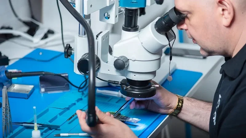
When you choose a way to make your microfluidic chip fixture, you have to decide between speed and accuracy. CNC machining gives you very tight limits and smooth surfaces. 3D printing gives you a part in hours for less money. The choice depends on where you are in development. For early versions of microfluidic chips, 3D printing saves time and money. For final microfluidic chip fixtures that need to seal well, CNC machining is the usual choice. Many teams use both methods. The way you make the fixture affects what materials you can use, how smooth the surface is, and how long it takes. The manufacturing methods you pick also affect cost and how easy it is to make more. Let’s look at each method.
CNC Machining for High Precision
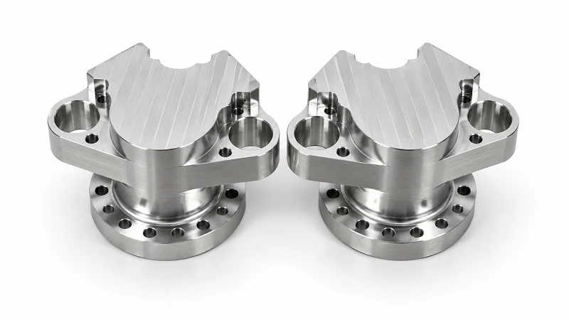
CNC machining cuts away material from a solid block using computer-controlled tools. This method gives you the best accuracy and surface finish. If your fixture needs to seal against O-rings or hold important sizes, CNC machining is the right pick. NOBLE’s precision machining services can make your microfluidic chip fixture with the tight limits needed for good performance.
Achieving Tight Tolerances in Metal
Metal fixtures need the tightest limits. For microfluidic ports and sealing surfaces, even small mistakes cause leaks. Micro CNC machining often holds size accuracy within ±0.0005 inches (±0.0127 mm). This level of precision directly affects how well your fixture seals. For even smaller features, micro CNC drilling can reach limits of ±1 micron. These numbers come from real production experience. When you machine in aluminum or stainless steel, you get the same results every time. The microfluidic chip fixture keeps its shape through many assembly cycles.
Machining Complex Geometries in Plastic
Plastic fixtures are lighter and sometimes cheaper than metal ones. But machining plastic needs different speeds and feed rates. Heat is the main problem. Plastic melts if the tool runs too fast. With the right settings, CNC machining makes clean features in PEEK, acrylic, and polycarbonate. The same accuracy standards apply. You can hold ±0.0005 inches in plastic too.
3D Printing for Rapid Prototyping
3D printing builds parts layer by layer. This method is fast and cheap for early design work. You can test a fixture, find problems, and print a new version the same day. But printed parts have limits. The surface finish is rougher than machined parts. Layer lines can create leak paths. Printed parts work best for checking fit and function, not for final use under pressure. NOBLE also offers 3D printing services for quick prototyping.
Stereolithography (SLA) for Detail
SLA uses a laser to harden liquid resin into solid plastic. The layer height can be as small as 25 microns. This gives you smooth surfaces and fine details. SLA is good for microfluidic chip fixtures with small features and complex shapes. But the resin is brittle. It can crack under clamping pressure. Use SLA parts for visual checks and low-pressure testing only.
Fused Deposition Modeling (FDM) for Concept Testing
FDM melts plastic filament and lays it down in layers. It is the cheapest and fastest 3D printing method. FDM parts are strong enough for handling and assembly checks. But the surface is rough, and layer lines create leak paths. FDM works well for testing the overall shape of your microfluidic chip fixture. Do not use it for pressure tests.
Surface Finishing and Post-Processing
The surface finish of your fixture decides how well it seals. For O-ring contact surfaces, you need a finish of 32 RMS or better. Both machined and printed parts can be improved with extra steps.
Polishing for Optical Clarity
If your microfluidic experiment needs a clear view of the chip, the fixture material must be see-through. Acrylic and polycarbonate are common choices. Two methods give you optical clarity.
| Technique | Key Features | Applicability | Optical Clarity |
| Flame Polishing | Uses heat to reflow the surface layer | External edges and surfaces only | Like glass, clear, 93%+ light passes through |
| Vapor Polishing | Uses solvent vapors to smooth surfaces | Internal channels and complex cavities | Clear on internal surfaces, very little light scattering |
Vapor polishing is especially useful for microfluidic experiments. It reaches internal channels that flame polishing cannot touch.
Applying Coatings for Friction Reduction
Coatings make your microfluidic chip fixture last longer. Hard anodizing on aluminum adds a wear-resistant surface. PTFE coatings reduce friction and improve chemical resistance. For stainless steel, electropolishing removes surface peaks and creates a smooth finish. These treatments help your fixture survive repeated use without sticking or rusting.
Assembly, Testing, and Validation of the Fixture

Integrating Fluidic Components
Installing Fittings and Tubing
Getting the connections right starts before you touch the microfluidic chip fixture. The interface between macro-scale pumps and micro-scale channels needs careful attention. Select connectors and pumps that work together as a system. This creates a robust link that keeps flow rates and pressures steady during your microfluidic experiments.
Proper priming prevents air bubbles from entering your chip. Air pockets disrupt flow and ruin results. Follow these steps for clean connections:
- Fill the syringe and tubing with liquid before connecting anything.
- Back-fill the tubing completely to remove trapped air.
- Connect the tubing to the chip port while a small amount of fluid spills out. This ensures an air-free connection.
This technique takes practice but pays off in consistent data. A bubble trapped at the interface can block an entire channel network.
Mounting the Microfluidic Chip
Place the chip gently into the nest pocket. The alignment pins guide it into position. Press down evenly across the surface. Tighten the screws in a star pattern, just like lug nuts on a car wheel. This spreads the clamping force evenly and prevents stress cracks.
Start with light pressure on all screws. Then go back and tighten each one in small increments. Check that the chip sits flat and does not rock. A rocking chip means uneven pressure and a likely leak path.
Conducting Leak Tests and Pressure Checks
Setting Up the Test Rig
Your test rig should mimic real experimental conditions. Connect the assembled fixture to your pressure source. Use the same tubing and fittings you plan for actual runs. Start with low pressure and watch for bubbles or drips.
In one leakage test of PDMS-based microfluidic chips bonded to SiO2/GaAs substrates, researchers applied increasing pressure to the system. The experimental setup’s maximum available pressure reached 8.5 bar (8500 mbar). At this pressure limit, the chips remained intact with no leakage at the bonded interface. This confirmed leakage-free performance up to that pressure level.
Your microfluidic chip fixture should handle similar scrutiny. Test at your maximum working pressure, not just your typical operating range.
Identifying and Fixing Leak Points
Leaks show up in predictable places. O-ring extrusion happens when the gland depth is too shallow. The rubber squeezes out under pressure. Thread stripping occurs when you over-tighten fittings. Both problems have simple fixes.
For O-ring issues, check the gland depth against your design specs. For stripped threads, replace the fitting and use a torque wrench next time. Document every leak and its solution. This record helps you improve future designs.
Validating Performance and Repeatability
Testing for Alignment Consistency
Mount and unmount the chip several times. After each cycle, check that the ports line up correctly. Use a microscope to verify alignment. Measure the same port positions each time. Consistent results mean your alignment features work properly.
Run this test with multiple chips from the same batch. Chip-to-chip variation should not change alignment. If it does, your pocket tolerance may be too tight or too loose.
Verifying Fluid Flow Rates
Flow rate verification confirms your fixture does not restrict or alter fluid movement. Pump a known volume through the system at a set pressure. Measure the output volume and time. Compare these numbers against your expected flow rate.
Repeat this test across several days and temperatures. This catches problems that appear only after thermal cycling or extended use. For complex assay protocols, consistent flow rates matter even more. Small variations compound over long experiments.
Document all test results. Include photos of leak points, pressure readings, and flow measurements. This documentation supports quality assurance and guides future design iterations. NOBLE can assist with assembly and validation of your microfluidic chip fixture to ensure reliability before you scale up production.
Partnering with NOBLE for Microfluidic Chip Fixture Manufacturing

Building a dependable microfluidic chip fixture takes more than cutting a metal block. You need smart engineering, material knowledge, and quality systems you can trust. NOBLE brings all of these together in one place. Their team works with many fixture materials—aluminum, stainless steel, PEEK, PTFE, and acrylic—so you get honest advice for your specific needs.
Full-Service Capabilities from Design to Assembly
Engineering Support for Fixture Optimization
NOBLE does more than machine parts. Their engineers check your design before production starts. They look for tolerance issues, sealing problems, and manufacturing concerns that could cause failures later. This design review catches small mistakes early, when they are cheap to fix. Material advice is part of the service too. If you are not sure whether PEEK or stainless steel works with your solvent, their team helps you choose based on your real working conditions.
Assembly help goes beyond the machining floor. NOBLE can add fittings, mount chips, and test the complete fixture assembly. For research teams without their own machining tools, this full-service approach removes a major hurdle. You send your chip specifications and receive a tested, ready-to-use microfluidic chip fixture.
Precision Machining and Finishing Services
NOBLE’s precision machining services handle both metal and plastic parts. Their CNC equipment holds tolerances within ±0.0005 inches (±0.0127 mm) for critical sealing surfaces. Surface finishing meets the 32 RMS requirement for O-ring contact areas. They also offer post-processing options like anodizing for aluminum, PTFE coatings to reduce friction, and electropolishing for stainless steel. These finishing steps make microfluidic chip fixtures last longer and work better during repeated mounting cycles.
Certifications and Quality Assurance
ISO 9001:2015 Certified Processes
ISO 9001:2015 certification means NOBLE follows documented quality management procedures. Every fixture goes through controlled steps for purchasing, production, and inspection. This standard ensures consistency across batches. When you order ten microfluidic chip fixtures or a hundred, each one meets the same specifications.
ISO 13485:2016 Compliance for Medical Devices
For microfluidic chips used in diagnostic or clinical applications, ISO 13485:2016 compliance matters. This standard sets stricter rules for medical device manufacturing. The table below shows key requirements and how they apply to fixture production:
| Requirement Area | Key ISO 13485:2016 Requirement for Fixture Manufacturing |
| Design & Development | Verification that equipment performs as defined in design inputs; validation on representative equipment |
| Purchasing | Supplier selection based on ability to meet requirements; regular performance assessment |
| Identification & Traceability | Unique product identity during all phases; documented procedures to maintain traceability |
| Corrective & Preventive Action (CAPA) | Analysis of processes to identify nonconformity sources; actions to prevent recurrence |
Process validation is another key part. If a manufacturing step cannot be fully checked through inspection alone, NOBLE validates it before production. This includes Installation Qualification (IQ), Operational Qualification (OQ), and Performance Qualification (PQ) for equipment. Staff training and documentation procedures support these validated processes. Re-validation criteria are defined under change control, so any process change triggers a fresh review.
Why Choose NOBLE for Your Microfluidics Project
Streamlining the Supply Chain
Working with one partner simplifies your whole project. NOBLE handles design review, material sourcing, machining, finishing, and assembly. You avoid coordinating multiple vendors and managing quality across different suppliers. This streamlined approach shortens lead times and reduces communication errors. For companies scaling from prototype to production, having a single accountable partner makes the transition smoother.
Ensuring High-Quality, Functional Fixtures
Quality assurance at NOBLE goes beyond certifications. Every fixture undergoes inspection before shipment. Dimensional checks verify critical features. Surface finish measurements confirm sealing surfaces meet specifications. Functional testing catches problems that dimensional inspection might miss. This attention to detail means your microfluidic experiments run reliably from the first use. When your research depends on leak-free connections and precise alignment, that reliability is worth the partnership.
Building a good microfluidic chip fixture takes more than just cutting parts. It needs careful planning at every step—from measuring chip sizes to testing the final setup. Each choice affects the next one. The material you pick changes how well it seals. The design affects how easy it is to make. How you build it decides if your experiments work well.
This step-by-step way lowers risk and makes development faster. You avoid expensive redesigns and annoying leaks. Your microfluidic tests give you reliable, steady data.
The process may seem hard, but you don’t have to learn every step alone. Working with NOBLE gives you expert help for your microfluidic chips. Their engineers handle design checks, precision machining, and putting things together. They help make your microfluidic ideas work well and fast. That partnership lets you focus on science, not hardware problems.
FAQ of Microfluidic Chip Fixture Manufacturing
What causes most leaks in microfluidic chip fixtures?
Most leaks happen because sealing surfaces are too rough or the O-ring groove is the wrong depth. A surface finish of 32 RMS or better stops leak paths. The groove depth should squeeze O-rings by 20% to 25% for a good seal.
How do I pick between metal and polymer fixture materials?
Choose the material based on your solvents and pressure needs. Aluminum machines fast and suits prototypes. PEEK resists most chemicals. PTFE handles almost anything but bends under pressure. Acrylic only works for water-based microfluidic tests.
Can I 3D print a microfluidic chip fixture for pressure testing?
Printed parts work for checking fit, not for pressure tests. Layer lines create paths for leaks. SLA resin turns brittle when clamped. Use CNC machining for any fixture that must seal against O-rings.
What surface finish do O-rings need?
O-ring contact surfaces need 32 RMS or better. Machined parts usually meet this standard. Printed parts need extra steps like vapor polishing to smooth layer lines before they can seal.
How tight should I tighten microfluidic chip fixture screws?
Tighten in a star pattern with small steps. Start light on all screws, then add more gradually. Watch for chip rocking, which means uneven pressure. Too much force cracks brittle glass chips.
Why does my PDMS chip not fit the pocket?
PDMS shrinks when it cures. Soft lithography causes size changes that differ between batches. Measure real microfluidic chips before designing the pocket. Add 0.1mm to 0.2mm space on each side for slip-fit mounting.
What dead volume should I target?
Lower is better for most assays. Match tubing inner diameter to port diameter. Machine a recessed pocket with radial microgrooves to remove external gaps. This gets dead volume under 5%.