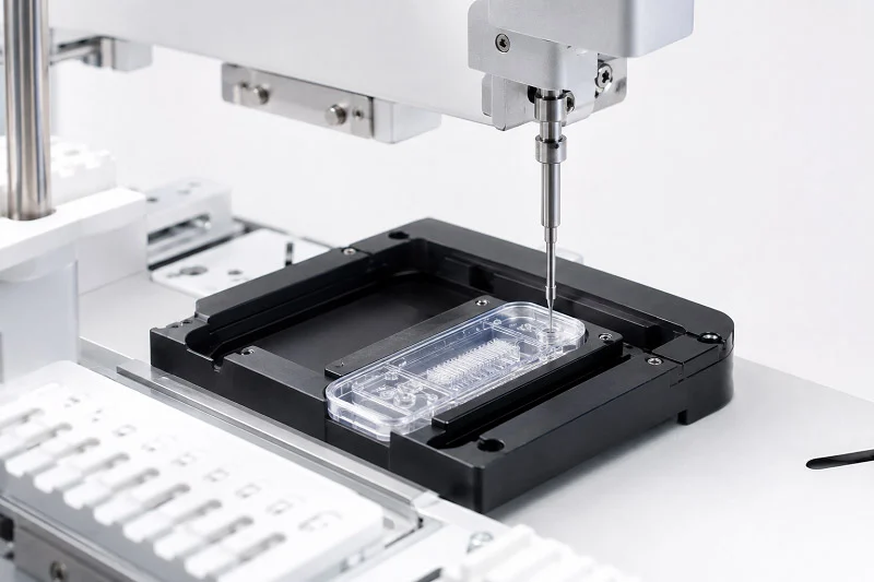
Lab-on-chip components are tiny devices that fit full lab functions onto one chip. The materials and manufacturing methods you choose affect performance, cost, and scalability. So which combination works best for your application? That question guides every decision, from prototyping to mass production.
The market shows why this matters. Global lab-on-chip devices reached about USD 6.01 billion in 2024, according to Spherical Insights, while Grand View Research reports the figure near USD 6.61 billion. Growth continues at a 9.5% CAGR from 2023 to 2033, says Market.us.
Think about your trade-offs carefully. The right fabrication route can speed up product development.
A poor material choice can slow down a promising lab-on-chip project.
Materials for Lab-on-Chip Components
Choosing materials for lab-on-chip components means finding a balance. You compare cost with precision, and flexibility with chemical resistance. Each choice affects your fabrication process and how well your final device works.
Polymers: Flexibility and Cost-Effectiveness in Microfluidics
Polymers are the top choice for microfluidics for good reason. They cost little, are simple to shape, and work great for quick prototyping.
Common Polymers (PDMS, PMMA, COC, PC)
PDMS (polydimethylsiloxane) is the go-to material in research labs. PMMA, COC, and PC are thermoplastics that work best in production. Each one adds its own benefits to microfluidic applications.
Advantages
| Low Cost | Polymer materials cost much less than glass or silicon. This is important when you’re making more lab-on-chip components. |
| Ease Of Prototyping | With PDMS, you can go from design to a working chip in hours. That speed changes how fast your research moves. |
| Optical Clarity | Most polymers let you see inside your channels. This is key for imaging and optical detection. |
Limitations
| Gas Permeability | PDMS lets gases pass through it. This is great for cell culture, but it causes problems for pressure-driven flow. |
| Limited Solvent Resistance | Many polymers swell or break down when they touch organic solvents. This limits what chemistry you can use. |
Glass and Silicon: High Precision and Chemical Resistance
Glass and silicon give you the opposite trade-off. You get precision and strength, but you pay more and work harder.
Substrate and Channel Fabrication
Fabrication methods for glass and silicon come from semiconductor processing. You use photolithography, etching, and bonding to build channels. For clear materials like glass, UV picosecond laser micromachining at 355 nm creates very little micro-cracking and gives sub-micron edge quality. Femtosecond laser micromachining, which uses ultra-short pulses in the 10⁻¹⁵ s range, allows high-precision, maskless processing with very small heat-affected zones and can reach sub-micron feature sizes. That makes it a good fit for 3D fabrication of micro-optical and microfluidic devices.
Advantages
| Thermal Stability | Glass and silicon can take high heat without changing shape. That opens the door to thermal cycling and sterilization. |
| Inertness | These materials stand up to most chemicals. Your device won’t leach into samples or react with them. |
| Established Microfabrication | Many years of semiconductor research give you proven methods. You’re not starting from scratch. |
Limitations
| Higher Cost | Material and processing costs are much higher than polymers. That hurts when you make large amounts. |
| More Complex Processing and Brittleness | Silicon is brittle and can crack under stress. Glass needs careful handling during bonding and dicing. |
Paper, Ceramics, and Hydrogels for Lab-on-Chip Components
Not every use needs a plastic or glass chip. Paper, ceramics, and hydrogels each solve their own problems.
Paper-based microfluidics for low-cost diagnostics
Paper-based devices are now a key tool for point-of-care diagnostics. They are tough and simple compared to channel microfluidics. Home pregnancy tests are the classic example. Researchers have also built a rapid POC nucleic acid amplification test that combines sample preparation and amplification using electrokinetics on paper substrates. This test uses simultaneous isotachophoresis and recombinase polymerase amplification to extract, amplify, and detect target nucleic acids from serum and whole blood in under 20 minutes, with low-cost materials. That makes it useful for finding infectious diseases and tracking viral infections in places with few resources.
| Application Area | Specific Examples |
| Lateral flow immunoassays | Home pregnancy tests |
| Nucleic acid amplification tests | Rapid POC NAAT for infectious diseases |
| Bodily fluid analysis | Urine, saliva, blood, tears |
| Early disease diagnosis | Dry eye disease, acute myocardial infarction |
| Integrated biomarker detection | CEA and AFP in serum using FICA-μPADs |
Ceramics and hydrogels for specific bio-applications
Hydrogels work best when you need a body-friendly environment. They use natural extracellular matrix proteins like collagen, fibrin, hyaluronic acid, Matrigel, fibronectin, agarose, and PEG diacrylate to copy the in vivo microenvironment. 3D structures in Matrigel, collagen type I, gelatin, and alginate boosted cell viability and lowered dedifferentiation. Microfluidic 3D culture of hepatocytes stayed functional for 4 weeks. Co-culture with feeder cells in alginate lasted up to 3 months, with better hepatic functions such as albumin secretion and urea synthesis. Pancreatic beta cells placed in PEG-based hydrogels showed viability climbing from 20% to 90%, with cells linking through E-cadherin junctions and keeping insulin secretion. Worries remain about whether enough body-friendly materials are available and whether microfluidic cell cultures can last long enough to give useful clinical results.
Hybrid material systems push these limits even more. A PDMS/PC/glass stack with four electrodes placed into microchannels allows direct TEER measurement and copies the blood-brain barrier for organ-on-a-chip work. A PDMS/polyester membrane/glass setup uses a porous membrane as a cell layer, with two separate layers for co-culture of gut epithelial and liver cells. Multi-layer PDMS/glass/porous membrane/PMMA designs put together five PDMS layers with screws and plasma bonding. 3D-printable PDMS-methacrylate macromers use stereolithography with 385 nm UV light and keep optical transparency, gas permeability, elasticity, and biocompatibility. Thermoplastic-based systems (PS, PC, COC) depend on laser ablation, injection molding, compression molding, and hot embossing for low cost, bio-inertness, and low intrinsic fluorescence.
Surface chemistry and biocompatibility tie all these choices together. A material might have high dimensional stability, but fail if proteins stick to it or cells won’t grow. Always test your material with your real sample before you commit to a production run.
Fabrication Processes for Lab-on-Chip Components
Choosing the right materials is only part of the job. You also need to shape them into working systems. The fabrication process you pick affects how long production takes and how good the device is. Some methods are great for quick prototypes. Others make low-cost parts in large amounts. Let’s go through the main techniques used in microfluidic chip fabrication today. These microfluidic techniques cover many different applications.
Molding Methods: Injection Molding, Hot Embossing, and Cold Casting
Molding methods copy a master pattern into a polymer substrate. They are the top choice for making the same part over and over in large amounts. The manufacturing method you pick depends on your production goals. The materials you use need to flow well when heated. Common materials include thermoplastics like PMMA and COC. The chip design affects how complex the tooling needs to be.
Cycle times, tooling costs, and replication fidelity
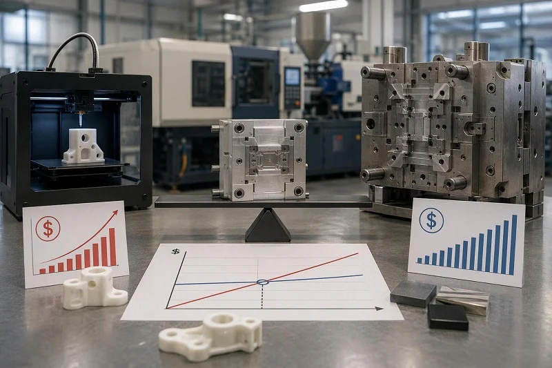
Injection molding works fast. You push melted thermoplastic into a steel mold. Each cycle finishes in seconds. The upfront cost is high — a good mold costs tens of thousands of dollars, and complex molds can go over $100,000. But that cost gets spread across every chip. Per-chip material costs drop to cents at scale. That’s why injection molding is the most cost-effective choice for thousands to millions of units.
Hot embossing sits in the middle. You press a heated mold into a polymer sheet. The setup is simpler. Cycle times run longer, and the process is less automated. Upfront cost is moderate. Hot embossing works well for medium volumes — hundreds to low thousands of lab-on-chip components.
For low-volume work with elastomeric materials like PDMS, casting methods using a master mold are employed. This approach is simple for small batches.
| Method | Upfront Cost | Per-Unit Cost at High Volume | Cycle Time |
| Injection Molding | High ($10k–$100k+) | Very low (cents to dollars) | Seconds per cycle |
| Hot Embossing | Moderate | Low to moderate | Longer than injection |
Suitable materials (thermoplastics, PDMS) and typical geometries
Injection molding and hot embossing work best with thermoplastics like PMMA, COC, PC, and PS. These materials flow well under heat and copy fine details with high fidelity. Many materials work well for microfluidic fabrication. Common shapes include straight channels, serpentine mixers, and droplet generators. The microfluidic chip geometry affects fluid flow. PDMS is naturally suited to casting methods, replicating features down to a few microns. Each material brings different strengths to microfluidic chip fabrication projects.
Prototyping Methods: Soft Lithography, 3D Printing, and Direct Machining
When you’re exploring a design, you don’t want expensive molds. Prototyping methods let you test ideas fast and cheap. Soft lithography is a key technique for early-stage work in microfluidic device fabrication.
Soft lithography with PDMS for rapid iteration in R&D
Soft lithography is the classic route for lab-on-chip devices. You start with a silicon master made by photolithography. Then you cast PDMS against it, peel off the cured layer, punch holes, and bond it to glass. The whole process takes a day or two. That speed makes soft lithography perfect for rapid iteration. Found a problem? Change the CAD file and cast a new chip.
PDMS remains popular because it’s easy to handle. It’s transparent, gas-permeable, and biocompatible. The trade-off is manual labor. Each chip needs individual attention, so soft lithography doesn’t scale to high volumes. Soft lithography is one of the most accessible techniques in microfluidic chip fabrication.
Micro-milling, laser ablation, and laser machining for custom designs
Direct machining gives you fine control. Micro-milling uses tiny cutting tools to carve channels into polymer or metal. It works well for complex 3D shapes and for making molds.
Laser ablation removes material with a focused beam. UV picosecond lasers at 355 nm produce channels with little micro-cracking and sub-micron edge quality. Femtosecond lasers use ultra-short pulses to machine with almost no heat damage. These techniques are maskless — you go from CAD to chip without photomasks.
3D printing has changed microfluidic prototyping by offering greater design flexibility and faster results. Researchers have used SLA printers to create molds for PDMS lab-on-chip components with high-resolution features. Other 3D printing systems can produce sealed fluidic devices using materials like COC. It can produce channel shapes that are difficult to achieve with etching.
Chip Bonding Techniques for Reliable Sealing
A chip needs a tight seal. Several bonding techniques are available. Bonding joins the channel layer to a substrate, creating closed channels without leaks. The right bonding technique depends on your materials. All these materials require compatible bonding approaches. The final step in microfluidic chip fabrication is often the most critical.
Thermal bonding, adhesive bonding, and anodic bonding
Thermal bonding heats a thermoplastic chip near its glass transition temperature and applies pressure. The layers fuse together. The risk is channel deformation if temperature isn’t controlled. This fabrication step is critical for quality.
Adhesive bonding uses a thin layer of glue. UV-curable adhesives cure at room temperature in seconds. The challenge is keeping adhesive out of the channels. These bonding techniques apply to many microfluidic devices.
Anodic bonding joins glass to silicon. You apply a high voltage across the interface at elevated temperature. The bond is strong, hermetic, and permanent. This technique comes from semiconductor processing. Each bonding technique suits different microfluidic applications.
Compatibility with different material pairs
The bonding method must match your materials. PDMS bonds to glass or itself after oxygen plasma treatment. Thermoplastics bond through thermal or solvent methods. Glass and silicon bond anodically. For hybrid systems — say a PDMS layer on glass — you might use plasma bonding or a thin adhesive.
Multi-material integration is growing. Emerging applications in diagnostics and drug delivery combine polymers, glass, and porous membranes in one chip. Each material pair needs its own bonding strategy. Get this wrong, and your chip leaks. Get it right, and the seal lasts the device’s lifetime. Proper material selection guides the entire fabrication process.
Designing Lab-on-Chip Components
Good design decides whether your lab-on-chip components work in the real world. Geometry, sensor placement, and cost all pull against each other. You can’t max out every factor at once.
Microfluidic Channel Geometry and Fluid Flow
Channel shape drives everything downstream. The top view, cross section, and longitudinal profile set the flow path. A smaller cross-sectional area builds pressure fast, and the relationship isn’t linear because of boundary layer effects. Length affects pressure. Flow rate follows the same linear rule.
Aspect ratio, turns, and dead volumes
Deep, narrow channels act differently than shallow, wide ones. Sharp turns create dead zones where fluid gets stuck. Those pockets hurt mixing and waste sample. Draft angle matters too, since it controls how straight the walls end up after fabrication. Stacking channels from wide to narrow helps spread flow evenly.
Impact on mixing, reaction kinetics, and separation efficiency
Longer channels raise pressure; reducing channel length reduces pressure accordingly. A two-layer mold with a larger cross section away from the junction can significantly reduce inlet pressure. Those gains matter for reaction kinetics and separation. Designers of microfluidic devices weigh these trade-offs all the time during microfluidic chip fabrication.
Integration of Sensors and Electrodes
Putting in electrodes sounds simple until you try it. Several problems show up fast:
- Wire bonding and solder bumps create surface bumps that fight the flat surface microfluidic channels need.
- CMOS lab-on-chip components take up only a few square millimeters, while channels, valves, and pumps need far more space.
- Placement registration error causes leaks, and side-to-side shift is hard to control.
- Up-and-down shift between chip and carrier can break both electrical and fluidic flow.
- Bonding the CMOS chip to microfluidic structures without leaks is still a real challenge.
- World-to-chip fluidic connections must seal in a reliable way.
Embedding electrodes for electrochemical detection
Electrochemical detection needs direct contact between sample fluid and electrodes. That touch demands a flat interface, which interconnect bumps mess up. Placing pads on two opposite sides helps a little, but yield stays low.
Alignment and packaging challenges
Precise alignment is a must for leak-free integration. Batch fabrication methods for multiple channels on CMOS haven’t been reported yet. These packaging hurdles shape how you approach microfluidic device fabrication.
Scalability and Cost Constraints
Cost scales in steps, not smoothly. At scale, injection molding requires significant upfront investment for the mold, but per-unit material costs drop to less than a dollar. Bulk molding pushes material cost below $1 per part. A small run through a service provider can cost significantly more per unit.
Design for manufacturability (DFM) principles
DFM means designing for the process you’ll really use. Avoid channels that are longer than they need to be. Keep draft angles the same. Plan bonding early, because material pairs limit your choices.
Balancing resolution, throughput, and unit cost
Higher resolution usually means slower cycles and pricier tooling. Polymer microfluidic lab-on-chip components trade some dimensional precision for speed and low unit cost. Glass gives finer features but lower throughput. Every microfluidic chip fabrication decision sits on that curve. These techniques serve diagnostics, drug delivery, and many other uses. Matching materials to uses early saves money later. The same logic applies across lab-on-chip devices of every type.
Scaling Lab-on-Chip Components Manufacturing
Scaling turns a working prototype into steady production. The path has many surprises. Let’s go through the main decisions.
Low-Volume Research vs. High-Volume Production
Going from a few lab-on-chip components to thousands changes everything. You need different materials, different tools, and different thinking.
When to choose prototyping methods vs. mass-production techniques
Small-scale methods like soft lithography work when the design keeps changing. You can test a new chip in a day. That speed helps researchers learn fast. But soft lithography doesn’t scale up. Each unit needs to be handled by hand. Mass-production methods like injection molding fit fixed designs. The upfront cost is high. Prototype tooling can cost tens of thousands of dollars. Hardened steel multi-cavity tools can cost $100,000 or more. Per-chip cost drops fast at high volume. The key is knowing when to switch. Use commercial mass production materials from the start. If you prototype with PDMS but use thermoplastics later, you face a redesign. Surface properties, gas permeability, and bonding methods all differ. Fix your material choice early to avoid rework.
Transition from soft lithography to injection molding
The transition takes time. Chip development involves multiple stages and can take several years. Intermediate-scale manufacturing helps bridge the gap. Family tools or soft aluminum tooling let you run near-industrial trials without paying for expensive steel molds. This phase reveals hidden problems. Material properties such as internal stress or autofluorescence can be affected by the molding process and must be evaluated. Catching these issues before final tooling saves money. A precision manufacturer with expertise in CNC machining and injection molding can support the transition from prototype to full production.
Trade-offs Between Resolution, Cost, and Throughput
No single material gives you everything. You trade one property for another. The trick is matching your choice to your application.
Material choice affects feature resolution and cycle time
Soft lithography with PDMS copies features as fine as 10 µm. That’s great for research. But PDMS doesn’t work for mass production. Thermoplastics work well for large-scale production but limit resolution at small scales. Glass and silicon reach sub-micrometer channel dimensions with high reproducibility. The trade-off is cost. Glass and silicon need expensive facilities and trained technicians.
Example trade-offs: glass (high resolution, low throughput) vs. polymer (lower resolution, high throughput)
Glass gives the finest features. Channels smaller than a micron are possible. The fabrication uses photolithography and dangerous chemicals. Throughput stays low. Cost per chip stays high.
Polymer lab-on-chip components trade some resolution for speed. Injection molding produces thousands of units per day. Features are larger — usually tens of microns. For many microfluidic applications, that resolution is enough. Lower cost lets you make disposable lab-on-chip devices.
Case Examples in Microfluidic Chips Manufacturing
Real microfluidic chip fabrication projects show how these choices play out.
Point-of-care diagnostic lab-on-chip components using injection-molded thermoplastics
A company developing a rapid diagnostic test chose injection-molded thermoplastics. The chip needed to be cheap enough for single use. The team fixed the material early — COC, a thermoplastic with good optical clarity. They designed for injection molding from the start. The upfront tooling cost was significant. Per-chip cost dropped below one dollar at volume. The final device works for point of care diagnostic applications where cost matters most. This microfluidic chip fabrication approach fits high-volume needs.
Research lab-on-chip components using PDMS and glass bonding
A university lab studying cell behavior chose a different path. They needed to test many designs quickly. PDMS soft lithography let them iterate fast. They bonded the PDMS layer to a glass slide using oxygen plasma. The lab-on-chip components were transparent, gas-permeable, and biocompatible. Each batch took a day to make. Cost per chip was higher. But the flexibility was worth it. For research, speed and iteration matter more than unit cost. This microfluidic chip fabrication method suits low-volume work.
These examples show how different applications demand different approaches. The right fabrication path depends on your volume, budget, and performance needs. Thinking about these trade-offs early helps you avoid costly mistakes later. Whether you need a few research prototypes or millions of production units, matching your fabrication strategy to your goals is the key to success.
NOBLE: Precision Manufacturing for Lab-on-Chip Components
Moving from a prototype to full production needs a partner who knows both steps. A manufacturer with expertise in metal and plastic processing can handle lab-on-chip making needs. Combining different methods streamlines the microfluidic chip building process, from design to assembly.
Comprehensive Metal and Plastic Processing Capabilities
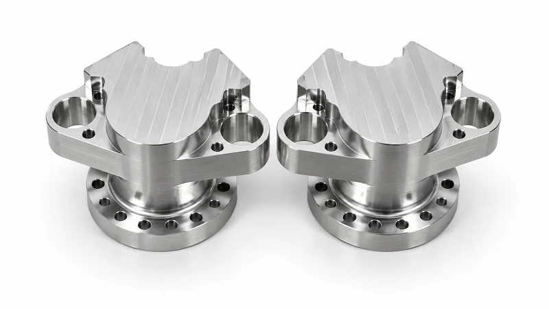
CNC machining, injection molding, and precision stamping
Machining approaches can accelerate early development. A micromilling process starts with a CAD model, makes toolpaths, and cuts parts right away. No master mold is needed.
Machining does not require a clean room, giving it an edge over soft lithography. This saves time and money for microfluidics work.
Capabilities include machining features suitable for droplet generators and mixing channels. Material choice matters: thermoplastics like PMMA, polycarbonate, and COC cut cleanly and retain optical clarity. Metals such as stainless steel, aluminum, and titanium are durable and chemically resistant.
| Material Type | Advantages | Surface Quality |
| Thermoplastics (PMMA, PC, COC) | Clean cuts, lower cost, optical clarity | PMMA gives mirror-like channels; COC has low autofluorescence |
| Metals (Steel, Aluminum, Titanium) | Durable, sterilizable, chemical-resistant | Needs extra polishing to match plastic smoothness |
A hybrid approach can combine 3D printing for complex internal geometries with machining for tight tolerances and smooth surfaces. Injection molding is suitable for high volumes, with hardened steel molds capable of long production runs. Per-part costs drop significantly at scale. These methods support a range of microfluidic lab-on-chip components.
Expertise in microfluidic mold design and micro-machining
Designing molds for microfluidics requires specialized knowledge. The mold surface must accurately replicate fine features across all cavities.
A skilled team designs molds that fill evenly and release cleanly, lasting through many cycles. Their micromachining capability allows test molds to be cut directly in metal, enabling design verification before scaling to production tools. This reduces risk when moving from prototype to volume.
Certifications and Quality Assurance
Certification for quality management
Quality management certification means a documented quality system is in place. Every step follows a defined workflow. This is important for microfluidic chip making, where small burrs or shape variations can affect channel sealing. Consistent quality leads to high production yields.
Certification for medical device applications
For lab-on-chip devices used in diagnostics or clinical applications, certification covering medical device quality systems is key. It addresses risk management, traceability, and process controls.
A full-service model — from design support to assembly — provides a single point of contact for the manufacturing process. Guidance on fabrication choices, materials, and bonding methods reduces communication errors and speeds product development.
No one material or making method works for all lab-on-chip devices. You choose materials based on cost, how the body reacts, and how many lab-on-chip components you need. Each making method has trade-offs between cost and accuracy. The best path depends on what you need and how much you can spend.
New trends such as automation, miniaturization, and AI-driven analysis create new options. New methods like additive manufacturing greatly change how you plan making. These advances help you match your microfluidic chip design exactly.
Your microfluidic chip needs a specific making method for scaling up. Contact a manufacturer for advice on making your microfluidic chip. Their team picks the right techniques for your chip’s use. They help with every step of making your microfluidic chip.
FAQ of Lab-on-Chip Components
Which material should I pick for my first lab-on-chip devices?
It depends on what you want to do. PDMS is great for quick prototypes. Thermoplastics like COC or PMMA work well for production runs. Glass and silicon give you the finest features. Test your material with real samples before you commit.
How do I choose between injection molding and soft lithography?
Soft lithography works for small batches and designs that change. Injection molding fits fixed designs at high volume. The upfront mold cost is high, but per-chip cost drops fast. Switch when your design stops changing.
What causes a microfluidic chip to leak?
Bad bonding is usually the problem. The bonding method must match your materials. PDMS bonds to glass after plasma treatment. Thermoplastics need thermal or solvent bonding. Glass and silicon bond anodically. A mismatched pair will fail.
Can I prototype with PDMS and then switch to plastic?
You can, but expect a redesign. Surface properties, gas permeability, and bonding methods all differ. Fix your material choice early. Prototyping with your production material saves rework later.
What feature size can each fabrication method achieve?
PDMS soft lithography copies features down to about 10 µm. Thermoplastics limit resolution at small scales. Glass and silicon reach sub-micrometer dimensions. Pick based on what your application actually needs.
Why does channel geometry matter so much?
Channel shape drives flow, mixing, and pressure. Sharp turns create dead zones. Longer channels raise pressure. A smaller cross section builds pressure fast. Good geometry keeps your microfluidic chip working as designed.
When should I move from prototype to mass production?
Move when your design is stable and volume grows. Prototype tooling costs less than hardened steel molds. Intermediate tooling bridges the gap. Watch for hidden problems like internal stress or changed autofluorescence before final tooling.
Does bonding affect the whole fabrication process?
Yes. Bonding is often the last step, and it can ruin everything before it. Each material pair needs its own strategy. Get it right, and the seal lasts the device’s lifetime. Get it wrong, and your microfluidic chip leaks.